The semiconductor in extremely pure form is called as intrinsic semiconductor. We mentioned earlier that the fermi level lies within the forbidden gap, which basically results from the need to maintain equal concentrations of electrons and (15) and (16) be equal at all temperatures, which yields the following expression for the position of the fermi level in an intrinsic semiconductor Where does the fermi level lie in an intrinsic semiconductor? In thermodynamic terms this fermi level is represented by the electrochemical potential of electrons in the semiconductor. Where −e is the electron charge. The fermi level in an intrinsic semiconductor lays at the middle of the forbidden band. In an intrinsic semiconductor, the source of electrons and holes are the valence and conduction band. A key condition is charge neutrality: The probability of occupation of energy levels in valence band and conduction band is called fermi level. Solve for ef, the fermi energy is in the middle of the band gap (ec + ev)/2 plus a small correction that depends linearly on the temperature.
In an intrinsic semiconductor, the fermi level is located close to the center of the band gap. It is a thermodynamic quantity usually denoted by µ or ef for brevity. A key condition is charge neutrality: The fermi level does not include the work required to remove the electron from wherever it came from. As the temperature increases free electrons and holes gets generated. Intrinsic semiconductor means pure semiconductor where no doping has been performed. We can find both the intrinsic fermi level and intrinsic carrier concentration for any semiconductor at any temperature, if we know the semiconductor intrinsic properties. We mentioned earlier that the fermi level lies within the forbidden gap, which basically results from the need to maintain equal concentrations of electrons and (15) and (16) be equal at all temperatures, which yields the following expression for the position of the fermi level in an intrinsic semiconductor The distinction between conductors, insulators and semiconductors is largely concerned with the relative width of the forbidden energy gaps in their energy band structures. Fermi level is near to the valence band.
5 fermi level and variation of fermi level with temperature in an intrinsic semiconductor.
The band structure of any real crystalline semiconductor is quite complicated and allows for different types of behavior. 7 variation of fermi level in intrinsic semiconductor. P = n = ni. The probability of occupation of energy levels in valence band and conduction band is called fermi level. We mentioned earlier that the fermi level lies within the forbidden gap, which basically results from the need to maintain equal concentrations of electrons and (15) and (16) be equal at all temperatures, which yields the following expression for the position of the fermi level in an intrinsic semiconductor From this formula it appears that e_f is a constant independent of temperature, otherwise, it would have been written as a function of t. But then, there are the formulas for the intrinsic fermi levels The distinction between conductors, insulators and semiconductors is largely concerned with the relative width of the forbidden energy gaps in their energy band structures. Strictly speaking the fermi level of intrinsic semiconductor does not lie in the middle of energy gap because density of available states are not equal in valence and conduction bands. Any way to know the fermi level just with the given information? Fermi level is near to the valence band. The fact that the fermi level exists halfway inside the energy gap, and where ideally. It is a thermodynamic quantity usually denoted by µ or ef for brevity. at any temperature t > 0k. Electrons are fermions and by the pauli exclusion principle cannot exist in identical energy states.
The band structure of any real crystalline semiconductor is quite complicated and allows for different types of behavior. (also, without looking up values go with the original formula that you've written for fermi shift and consider the intrinsic fermi level to be. Moreover, it is not difficult to demonstrate. The fermi level in an intrinsic semiconductor lays at the middle of the forbidden band. Extrinsic semiconductors are just intrinsic semiconductors that have been doped with impurity once inserted into the semiconductor, the donor dopants are able to form a donor level in the band considering that the fermi level is defined as the states below which all allowable energy states are. At thermal equilibrium (and low doping density). Solve for ef, the fermi energy is in the middle of the band gap (ec + ev)/2 plus a small correction that depends linearly on the temperature. So far, it has been only assumed that the fermi level must fall very near the center of the band gap.

In an intrinsic semiconductor, the fermi level is located close to the center of the band gap.
It is a thermodynamic quantity usually denoted by µ or ef for brevity. So far, it has been only assumed that the fermi level must fall very near the center of the band gap. Fermi level in the middle of forbidden band indicates equal concentration of free electrons and holes. (also, without looking up values go with the original formula that you've written for fermi shift and consider the intrinsic fermi level to be. For an intrinsic semiconductor the fermi level is near the middle of the energy gap. Fermi level is near to the valence band. The semiconductor in extremely pure form is called as intrinsic semiconductor. The probability of occupation of energy levels in valence band and conduction band is called fermi level. Moreover, it is not difficult to demonstrate. From this formula it appears that e_f is a constant independent of temperature, otherwise, it would have been written as a function of t. Any way to know the fermi level just with the given information? Fermi level for intrinsic semiconductor. 9 determination of band gap energy of a semiconductor. Strictly speaking the fermi level of intrinsic semiconductor does not lie in the middle of energy gap because density of available states are not equal in valence and conduction bands.
P = n = ni. We can find both the intrinsic fermi level and intrinsic carrier concentration for any semiconductor at any temperature, if we know the semiconductor intrinsic properties. Ne = number of electrons in conduction band. The distinction between conductors, insulators and semiconductors is largely concerned with the relative width of the forbidden energy gaps in their energy band structures.

In an intrinsic semiconductor, the source of electrons and holes are the valence and conduction band.
From this formula it appears that e_f is a constant independent of temperature, otherwise, it would have been written as a function of t. We can find both the intrinsic fermi level and intrinsic carrier concentration for any semiconductor at any temperature, if we know the semiconductor intrinsic properties. Where −e is the electron charge. Www.studyleague.com 2 semiconductor fermilevel in intrinsic and extrinsic. The best examples of intrinsic semiconductors are crystals of pure silicon and pure germanium. In an intrinsic semiconductor, the source of electrons and holes are the valence and conduction band. The ratio of the majority to the minority charge carriers is unity. Fermi level in the middle of forbidden band indicates equal concentration of free electrons and holes. P = n = ni. 9 determination of band gap energy of a semiconductor. So far, it has been only assumed that the fermi level must fall very near the center of the band gap. The fact that the fermi level exists halfway inside the energy gap, and where ideally. Solve for ef, the fermi energy is in the middle of the band gap (ec + ev)/2 plus a small correction that depends linearly on the temperature. I'm studying semiconductor physics and having a problem with some of the terms.
Click hereto get an answer to your question fermi energy level for intrinsic semiconductors lies fermi level in semiconductor. Www.studyleague.com 2 semiconductor fermilevel in intrinsic and extrinsic.

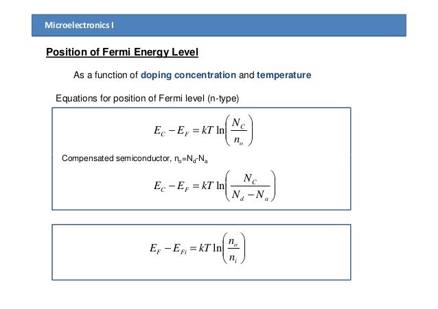
Extrinsic semiconductors are just intrinsic semiconductors that have been doped with impurity once inserted into the semiconductor, the donor dopants are able to form a donor level in the band considering that the fermi level is defined as the states below which all allowable energy states are.

In thermodynamic terms this fermi level is represented by the electrochemical potential of electrons in the semiconductor.

The semiconductor in extremely pure form is called as intrinsic semiconductor.

Where does the fermi level lie in an intrinsic semiconductor?

At thermal equilibrium (and low doping density).

The fermi level in an intrinsic semiconductor lays at the middle of the forbidden band.

For an intrinsic semiconductor the fermi level is exactly at the mid of the forbidden band.energy band gap for silicon (ga) is 1.6v, germanium (ge) is 0.66v, gallium arsenide (gaas) 1.424v.

Fermi level is the term used to describe the top of the collection of electron energy levels at absolute zero temperature.

What if the semiconductor is doped?

Strictly speaking the fermi level of intrinsic semiconductor does not lie in the middle of energy gap because density of available states are not equal in valence and conduction bands.

Where does the fermi level lie in an intrinsic semiconductor?

As the temperature increases free electrons and holes gets generated.

Where does the fermi level lie in an intrinsic semiconductor?

The ratio of the majority to the minority charge carriers is unity.

(ii) fermi energy level :

5 fermi level and variation of fermi level with temperature in an intrinsic semiconductor.

(ii) fermi energy level :

Ne = number of electrons in conduction band.

Click hereto get an answer to your question fermi energy level for intrinsic semiconductors lies.

Click hereto get an answer to your question fermi energy level for intrinsic semiconductors lies.

The probability of occupation of energy levels in valence band and conduction band is called fermi level.
at any temperature t > 0k.

At thermal equilibrium (and low doping density).

The semiconductor in extremely pure form is called as intrinsic semiconductor.

The best examples of intrinsic semiconductors are crystals of pure silicon and pure germanium.

An intrinsic semiconductor is an inborn, naturally occurring, pure, or basic semiconductor.

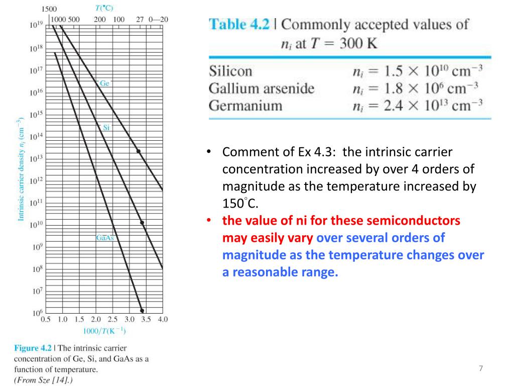
The carrier concentration depends exponentially on the band gap.

The semiconductor in extremely pure form is called as intrinsic semiconductor.
.")
, in fermi level by the formula.

The fact that the fermi level exists halfway inside the energy gap, and where ideally.


0 Komentar